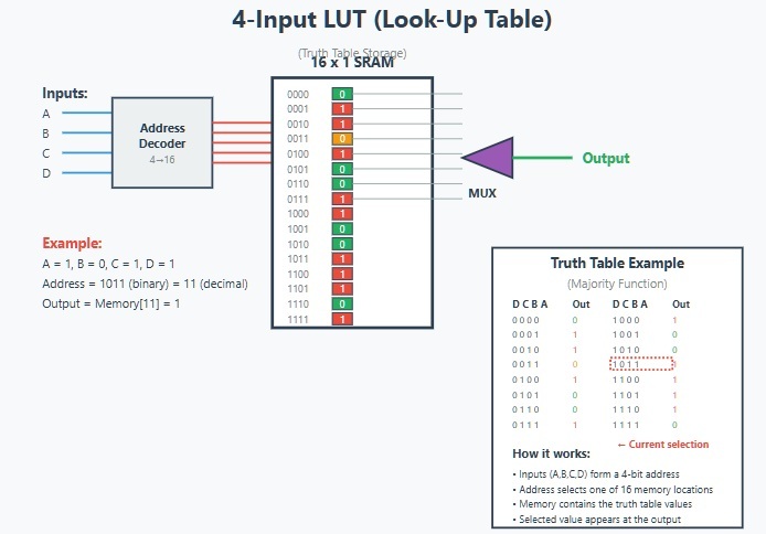
Structure:
- Inputs (A, B, C, D): The 4 input signals that form a binary address
- Address Decoder: Converts the 4-bit input into a selection signal for one of 16 memory locations
- 16 x 1 SRAM: The memory array that stores the truth table values (one bit for each possible input combination)
- Output Multiplexer: Selects and outputs the value from the addressed memory location
Operation:
- The 4 inputs create a 4-bit binary address (0000 to 1111)
- This address selects one of the 16 stored values in the SRAM
- The selected value appears at the output
- The example shows inputs A=1, B=0, C=1, D=1 (address 1011 = 11 decimal) producing output 1
Truth Table: The diagram includes a sample truth table implementing a majority function, where the output is 1 when the majority of inputs are 1. The memory cells are color-coded to match the truth table values.
This diagram helps visualize how LUTs can implement any 4-input Boolean function by simply storing the desired output values in the internal memory. During FPGA configuration, the synthesis tools determine what values to store in each LUT’s memory to implement the desired logic function.
